
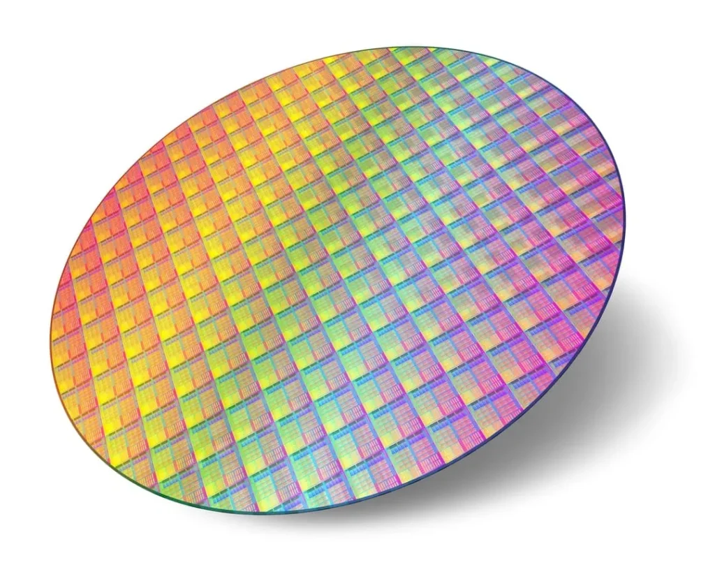
Modern electronics — from AI accelerators to medical sensors — rely on vertical connections drilled through silicon wafers, called Through-Silicon Vias (TSVs). Today these are made with a slow, chemistry-heavy process called Deep Reactive Ion Etching (DRIE). DRIE leaves rough, scalloped walls that limit electrical performance and require multiple additional treatment steps.
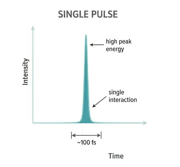
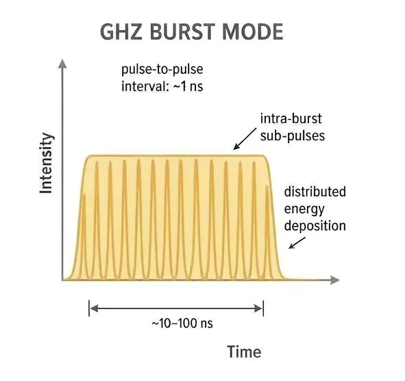
STAY2ME’s proposed solution — a directly-emitting holmium-doped crystal laser at 2.1 µm in GHz-burst mode — is chosen because holmium uniquely combines high pulse energy storage, stable burst amplification, and a wavelength perfectly matched to silicon’s transparency window.